|
Product Details:
|
| Material: | FR-4 | Color: | Green, Customized Color, Blue On Your Request |
|---|---|---|---|
| Copper Thickness: | 1oz,0.5-2.0 Oz,1-3oz,0.5-5oz,0.5-4oz | Board Thickness: | 1.6mm, |
| Min. Line Width: | 3mi, 4mil, 0.1mm, 0.1mm(Flash Gold)/0.15mm(HASL), 0.1 0mm | Application: | Electronics Device, Consumer Electronics, Electronical Products, Industrial, And So On |
| High Light: | FR4 Multilayer Pcb Fabrication Process,FR4 Three Layer Pcb,1.6mm Printed Circuit Board |
||
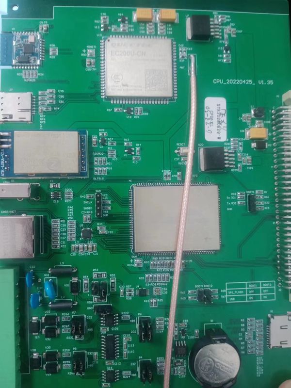
SMT (short for Surface Mounted Technology) is one of the most popular technologies and processes in the electronic assembly industry. Surface Mount Technology (SMT) of electronic circuits is called surface mount or surface mount technology. It is a kind of pin-free or short-lead surface assembly components (SMC/SMD, Chinese known as chip components) installed on the Printed Circuit Board (PCB) surface or other substrate surface, through reflow welding or immersion welding and other methods to be welded and assembled circuit installation technology.
Advantages of single layer circuit board
(1) Low cost: The manufacturing cost of single-layer PCB board is relatively low, because only one layer of copper foil and one layer of substrate are needed, and the manufacturing process is relatively simple.
(2) Easy production: Compared with other structural types of PCB board, the production method of single-layer PCB board is relatively simple, only need to carry out single-side wiring and single-layer corrosion, so the production difficulty is low.
(3) High reliability: Single-layer PCB board does not have multi-layer wiring and connection, so it is not easy to short-circuit and interference problems, with high reliability.
(4) Suitable for simple circuit: single-layer PCB board is suitable for simple circuit design, such as LED lights, sound, etc., can meet most of the low complexity of the circuit requirements.
| Copper Thickness | 1oz~3oz,0.5-5 Oz | Base Material | FR4, Aluminium, TG, Rogers, CEM-1 |
| Board Thickness | 1.6mm, 0.5~3.2mm, 0.2-3.0mm, 0.3~2.5mm, 2.0mm | Min. Line Width | 3mi, 4mil, 0.1mm, 0.1mm(Flash Gold)/0.15mm(HASL), 0.1 0mm |
| Min. Hole Size | 0.25mm, 0.1mm, 0.2 Mm, 0.15-0.2mm, 0.1mm-1mm | Surface Finishing | HASL, OSP, ENIG, HASL Lead Free, Immersion Gold |
| Min. Line Spacing | 0.003", 4mil, 0.2mm, 0.15mm, 0.1mm4mil) | Product Name | Printed Circuit Board, 94V0 PCB Design / PCB Manufacturing |
| Application | Electronics Device, Consumer Electronics, Electronical Products, Industrial, And So On | Solder Mask | Blue, Green. Red. Blue. White. Black.Yellow, Green/black/white/red/blue Etc., |
| Layer | 1~20 Layers, 1-24layers | Rohs | Lead free |
Q: What files do you use in PCBA fabrication?
A: Gerber or Eagle, BOM listing, PNP and Components Position.
Q: Is it possible you could offer sample?
A: Yes, we can custom samples for your testing before mass production.
Q: How much time could I get the quotation after sent Gerber, BOM and test procedure?
A: Within 6 hours for PCB quotation and around 24 hours for PCBA quotation.
Q: How can I know the process of my PCBA production?
A: 7-10 days for PCB production and components purchasing, and 10 days for PCB assembly and Testing.
Q. Are my design secure when I send them to you?
Your files are held in complete safety and security while Kerongda is in possession of them.Your files are never shared with any third parties,only our colleagues have access to your design files.Since they are your property,we respect the copyright of your files.The customer controls the disposition of these files per your requirements and written approval.
Q.What is the warranty?
The warranty is 2years.
![]()
![]()
![]()
Contact Person: Wang
Tel: 18006481509