|
Product Details:
|
| Board Thickness: | 1.6mm, 0.5~3.2mm, 0.2-3.0mm, 0.3~2.5mm, 2.0m | Copper Thickness: | 1oz,0.5-2.0 Oz,1-3oz,0.5-5oz,0.5-4oz |
|---|---|---|---|
| Base Material: | FR-4, CEM-3, Aluminum, CEM-1 OR FR-4, Alum | Application: | Electronics Device, Consumer Electronics, Electronical Products, Industrial, And So On |
| Color: | Green, Customized Color, Blue On Your Request | Standards: | IPC-A-610 E Class II-III, IPC 6021 Class 2, TDR Testing, ISO 9001, Class 3 |
| Min. Line Width: | 3mi, 4mil, 0.1mm, 0.1mm(Flash Gold)/0.15mm(HASL), 0.1 0mm | Min. Hole Size: | 0.25mm, 0.1mm, 0.2 Mm, 0.15-0.2mm, 0.1mm-1mm |
| High Light: | 1.6mm Double Sided Pcb,Cnc Double Layer Pcb,FR4 Dual Sided Pcb |
||
SMT basic process elements include: screen printing (or dispensing), mounting (curing), reflow soldering, cleaning, testing, repair
1. Screen printing: Its function is to leak solder paste or patch glue onto the PCB pad to prepare for the welding of components. The equipment used is screen printing machine (screen printing machine), located at the front end of the SMT line.
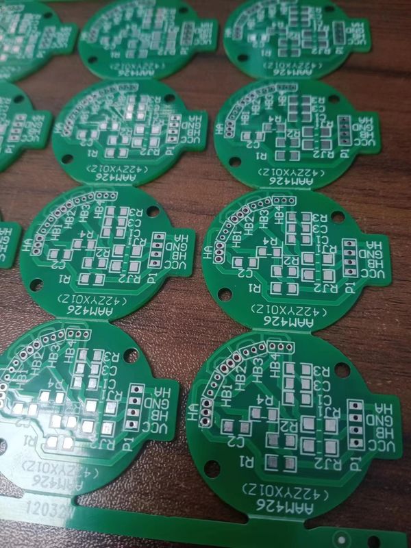
Double-sided PCB board
Double-sided PCB board is a very important PCB board in the circuit board, the market has double-sided circuit board metal base PCB board, Hi-Tg heavy copper foil circuit board, flat winding double-sided circuit board, high frequency PCB, mixed dielectric base high frequency double-sided circuit board, etc. It is suitable for a wide range of high-tech industries such as: telecommunications, power supply, computer, industrial control, digital products, scientific and educational instruments, medical instruments, automobiles, aerospace defense and so on.
| Copper Thickness | 1oz~3oz,0.5-5 Oz |
| Board Thickness | 1.6mm, 0.5~3.2mm, 0.2-3.0mm, 0.3~2.5mm, 2.0mm |
| Min. Hole Size | 0.25mm, 0.1mm, 0.2 Mm, 0.15-0.2mm, 0.1mm-1mm |
| Min. Line Spacing | 0.003", 4mil, 0.2mm, 0.15mm, 0.1mm4mil) |
| Application | Electronics Device, Consumer Electronics, Electronical Products, Industrial, And So On |
| Layer | 1~20 Layers, 1-24layers |
| Base Material | FR4, Aluminium, TG, Rogers, CEM-1 |
| Min. Line Width | 3mi, 4mil, 0.1mm, 0.1mm(Flash Gold)/0.15mm(HASL), 0.1 0mm |
| Surface Finishing | HASL, OSP, ENIG, HASL Lead Free, Immersion Gold |
| Product Name | Printed Circuit Board, 94V0 PCB Design / PCB Manufacturing |
| Solder Mask | Blue, Green. Red. Blue. White. Black.Yellow, Green/black/white/red/blue Etc., |
| Rohs | Lead free |
Our Advantages:
1. Program and functional test and package by Free.
2. High quality: IPC-A-610E standard, E-test, X-ray, AOI test, QC, 100% functional test.
3. Professional service: PCB/FPC/Aluminium Making, SMT, DIP, Component Sourcing, OEM with 21 years experience.
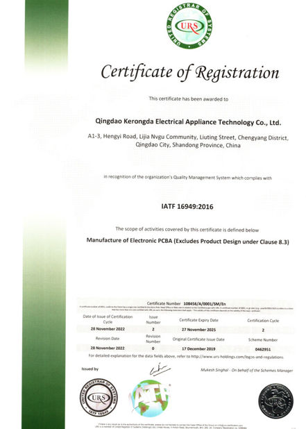
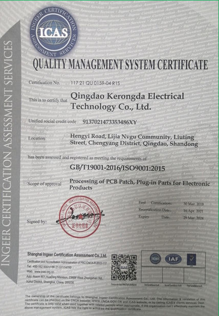
4. Certifications: UL, 94v-0, CE, SGS, FCC, RoHS, ISO9001, ISO14001,IATF16949
Q: What files do you use in PCBA fabrication?
A: Gerber or Eagle, BOM listing, PNP and Components Position.
Q: Is it possible you could offer sample?
A: Yes, we can custom samples for your testing before mass production.
Q: How much time could I get the quotation after sent Gerber, BOM and test procedure?
A: Within 6 hours for PCB quotation and around 24 hours for PCBA quotation.
Q: How can I know the process of my PCBA production?
A: 7-10 days for PCB production and components purchasing, and 10 days for PCB assembly and Testing.
Q. Are my design secure when I send them to you?
Your files are held in complete safety and security while Kerongda is in possession of them.Your files are never shared with any third parties,only our colleagues have access to your design files.Since they are your property,we respect the copyright of your files.The customer controls the disposition of these files per your requirements and written approval.
Q.What is the warranty?
The warranty is 2years.
![]()
![]()
![]()
![]()
Kerongda is a PCB manufacturer, providing turnkey and partial turnkey printed circuit board assembly services.We can produce customized PCB board and PCBA for you ,PCB solder mask color ,material, thickness etc... all can be chosed as your demands.
Contact Person: Wang
Tel: 18006481509