|
Product Details:
|
| Copper Thickness: | 1oz,0.5-2.0 Oz,1-3oz,0.5-5oz,0.5-4oz | Base Material: | FR4, Aluminium, TG, Rogers, CEM-1 |
|---|---|---|---|
| Board Thickness: | 1.6mm, 0.5~3.2mm, 0.2-3.0mm, 0.3~2.5mm, 2.0mm | Min. Line Width: | 3mi, 4mil, 0.1mm, 0.1mm(Flash Gold)/0.15mm(HASL), 0.1 0mm |
| Min. Hole Size: | 0.25mm, 0.1mm, 0.2 Mm, 0.15-0.2mm, 0.1mm-1mm | Surface Finishing: | HASL, OSP, ENIG, HASL Lead Free, Immersion Gold |
| Min. Line Spacing: | 0.003", 4mil, 0.2mm, 0.15mm, 0.1mm4mil) | Product Name: | Printed Circuit Board, 94V0 PCB Design / PCB Manufacturing / PCB Assembly In China, Double Sided PCB, 2 Layer HASL 94V0 FR4 PCB Manufacturer, Electronic Pcb Assembly |
| High Light: | low volume pcb manufacturer,single layer pcb manufacturer,pcb keypad manufacturer |
||
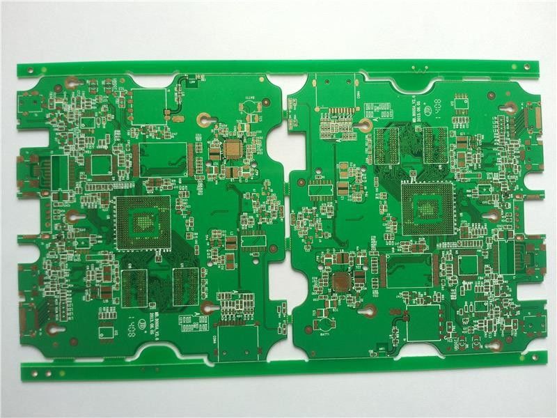
Advantages of multilayer circuit boards
1, the multi-layer circuit board assembly density is high, the size is small, with the volume of electronic products is getting smaller and smaller, the function of PCB circuit board is also put forward higher requirements, the demand for multi-layer circuit board is also increasing.
2, the selection of multi-layer PCB circuit board laying line is convenient, the length of the laying line is greatly shortened, the laying line between the electronic components is reduced, but also improve the data signal transmission rate.
3. For the high-frequency circuit, after entering the ground, the signal line has a stable and low characteristic impedance to the ground, and the characteristic impedance of the power circuit is greatly reduced, which has a significant intercepting effect.
4. For electronic products with higher requirements for heat dissipation function, metal core heat dissipation layer can be set up on multi-layer circuit board, which is convenient to satisfy the requirements of shielding, heat dissipation and other special functions.
| Copper Thickness | 1oz~3oz,0.5-5 Oz |
| Board Thickness | 1.6mm, 0.5~3.2mm, 0.2-3.0mm, 0.3~2.5mm, 2.0mm |
| Min. Hole Size | 0.25mm, 0.1mm, 0.2 Mm, 0.15-0.2mm, 0.1mm-1mm |
| Min. Line Spacing | 0.003", 4mil, 0.2mm, 0.15mm, 0.1mm4mil) |
| Application | Electronics Device, Consumer Electronics, Electronical Products, Industrial, And So On |
| Layer | 1~20 Layers, 1-24layers |
| Base Material | FR4, Aluminium, TG, Rogers, CEM-1 |
| Min. Line Width | 3mi, 4mil, 0.1mm, 0.1mm(Flash Gold)/0.15mm(HASL), 0.1 0mm |
| Surface Finishing | HASL, OSP, ENIG, HASL Lead Free, Immersion Gold |
| Product Name | Printed Circuit Board, 94V0 PCB Design / PCB Manufacturing |
| Solder Mask | Blue, Green. Red. Blue. White. Black.Yellow, Green/black/white/red/blue Etc., |
| Rohs | Lead free |
Why choose us?
1. Program and functional test and package by Free.
2. High quality: IPC-A-610E standard, E-test, X-ray, AOI test, QC, 100% functional test.
3. Professional service: PCB/FPC/Aluminium Making, SMT, DIP, Component Sourcing, OEM with 21 years experience.
4. Certifications: UL, 94v-0, CE, SGS, FCC, RoHS, ISO9001, ISO14001,IATF16949
Q: What files do you use in PCBA fabrication?
A: Gerber or Eagle, BOM listing, PNP and Components Position.
Q: Is it possible you could offer sample?
A: Yes, we can custom samples for your testing before mass production.
Q: How much time could I get the quotation after sent Gerber, BOM and test procedure?
A: Within 6 hours for PCB quotation and around 24 hours for PCBA quotation.
Q: How can I know the process of my PCBA production?
A: 7-10 days for PCB production and components purchasing, and 10 days for PCB assembly and Testing.
Q. Are my design secure when I send them to you?
Your files are held in complete safety and security while Kerongda is in possession of them.Your files are never shared with any third parties,only our colleagues have access to your design files.Since they are your property,we respect the copyright of your files.The customer controls the disposition of these files per your requirements and written approval.
Q.What is the warranty?
The warranty is 2years.
![]()
![]()
![]()
Contact Person: Wang
Tel: 18006481509