|
Product Details:
|
| Copper Thickness: | 1oz,0.5-2.0 Oz,1-3oz,0.5-5oz,0.5-4oz | Min. Line Width: | 3mi, 4mil, 0.1mm, 0.1mm(Flash Gold)/0.15mm(HASL), 0.1 0mm |
|---|---|---|---|
| Min. Hole Size: | 0.25mm, 0.1mm, 0.2 Mm, 0.15-0.2mm, 0.1mm-1mm | Surface Finishing: | HASL, OSP, ENIG, HASL Lead Free, Immersion Gold |
| Application: | Electronics Device, Consumer Electronics, Electronical Products, Industrial, And So On | Layers: | 1-58layers, 1-32, 1-48 |
| Solder Mask: | Blue, Green. Red. Blue. White. Black.Yellow | Item: | ODM OEM LED PCBA, 2 Layer Pcb, Keyboard Pcb Assembly, Custom Circuit Board |
| High Light: | smd board assembly,smd pcb assembly,assembly smt |
||
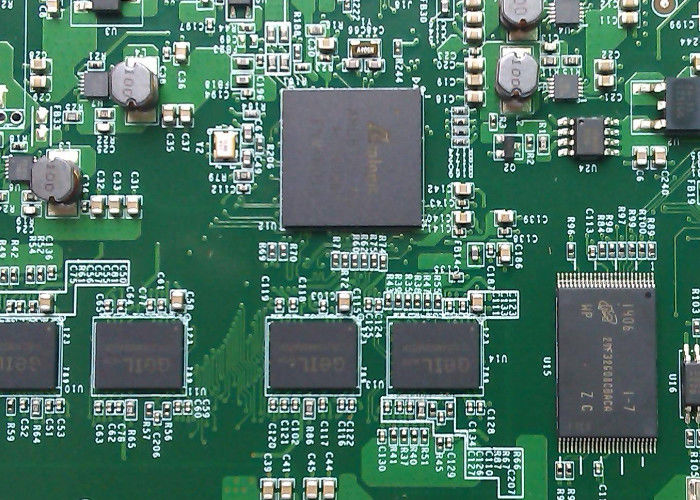
SMT/Dip/Oem pcba/Kerongda/Smt Control pcb/Multilayer board
SMT basic process elements include: screen printing (or dispensing), mounting (curing), reflow soldering, cleaning, testing, repair
1. Screen printing: Its function is to leak solder paste or patch glue onto the PCB pad to prepare for the welding of components. The equipment used is screen printing machine (screen printing machine), located at the front end of the SMT line.
2, dispensing: it is to drop the glue to the fixed position of the PCB board, its main role is to fix the components to the PCB board. The equipment used is the dispensing machine, which is located at the front end of the SMT production line or behind the testing equipment.
3. Mounting: Its function is to accurately install the surface assembly components to the fixed position of PCB. The equipment used is the SMT machine, which is located behind the screen printing machine in the SMT production line.
4, curing: its role is to melt the patch glue, so that the surface assembly components and PCB board firmly bonded together. The equipment used is the curing furnace, which is located behind the SMT machine in the SMT line.
5, reflow welding: its role is to melt the welding paste, so that the surface assembly components and PCB board firmly bonded together. The equipment used is reflow furnace, which is located behind the SMT machine in the SMT line.
6, cleaning: its role is to assemble the PCB board above the welding residue harmful to human health, such as flux, etc., to remove. The equipment used is a cleaning machine, the position can not be fixed, can be online or not online.
7, detection: its role is to assemble the PCB board welding quality and assembly quality detection. The equipment used includes magnifying glass, microscope, online tester (ICT), flying needle tester, automatic optical testing (AOI), X-RAY testing system, function tester, etc. Location According to the need of detection, can be configured in the production line of the appropriate place.
8, repair: its role is to detect the fault of the PCB board rework. The tools used are soldering iron, repair workstation, etc. Configuration anywhere in the production line.
Single-side mixed loading process
Incoming material detection => PCB side A screen printing solder paste (spot patch glue) => patch => drying (curing) => reflow welding => cleaning => plug-in => wave soldering => cleaning => detection => repair
Double-sided mixed loading process
A: Incoming material detection =>PCB B spot patch glue => patch => curing => turn over =>PCB A side plug-in => wave soldering => cleaning => detection => repair
Stick before insert, suitable for SMD components more than separate components
B: Incoming material detection => PCB side A plug-in (pin bent) => turn over => PCB side B patch glue => patch => curing => turn over => wave soldering => cleaning => detection => repair
Insert before paste, suitable for separated components more than SMD components
SMT basic process elements include: screen printing (or dispensing), mounting (curing), reflow soldering, cleaning, testing, repair
1. Screen printing: Its function is to leak solder paste or patch glue onto the PCB pad to prepare for the welding of components. The equipment used is screen printing machine (screen printing machine), located at the front end of the SMT line.
2, dispensing: it is to drop the glue to the fixed position of the PCB board, its main role is to fix the components to the PCB board. The equipment used is the dispensing machine, which is located at the front end of the SMT production line or behind the testing equipment.
DIP
1,The process of DIP processing is: putting in the hole →AOI→ wave soldering → cutting pin →AOI→ correction → washing → quality inspection.
2,After wave soldering, The products will be will scanned by AOI equipment to ensure that no error occurs.
| Turnkey PCBA | PCB+components sourcing+assembly+package | ||||
| Assembly details | SMT and Thru-hole, ISO lines | ||||
| Lead Time | Prototype: 15 work days. Mass order: 20~25 work days | ||||
| Testing on products | Flying Probe Test, X-ray Inspection, AOI Test, functional test | ||||
| Quantity | Min quantity: 1pcs. Prototype, small order, mass order, all OK | ||||
| Files we need | PCB: Gerber files(CAM, PCB, PCBDOC) | ||||
| Files we need | Components: Bill of Materials(BOM list) | ||||
| Files we need | Assembly: Pick-N-Place file | ||||
| PCB panel Size | Min size: 0.25*0.25 inches(6*6mm) | ||||
| Max size: 20*20 inches(500*500mm) | |||||
| PCB Solder Type | Water Soluble Solder Paste, RoHS lead free | ||||
| Components details | Passive Down to 0201 size | ||||
| Components details | BGA and VFBGA | ||||
| Components details | Leadless Chip Carriers/CSP | ||||
| Components details | Double-sided SMT Assembly | ||||
| Components details | Fine Pitch to 0.8mils | ||||
| Components details | BGA Repair and Reball | ||||
| Components details | Part Removal and Replacement | ||||
| Component package | Cut Tape,Tube,Reels,Loose Parts | ||||
| PCB assembly | Drilling-----Exposure-----Plating-----Etaching & Stripping-----Punching-----Electrical Testing-----SMT-----Wave Soldering-----Assembling-----ICT-----Function Testing-----Temperature & Humidity Testing | ||||
Q: What files do you use in PCBA fabrication?
A: Gerber or Eagle, BOM listing, PNP and Components Position.
Q: Is it possible you could offer sample?
A: Yes, we can custom samples for your testing before mass production.
Q: How much time could I get the quotation after sent Gerber, BOM and test procedure?
A: Within 6 hours for PCB quotation and around 24 hours for PCBA quotation.
Q: How can I know the process of my PCBA production?
A: 7-10 days for PCB production and components purchasing, and 10 days for PCB assembly and Testing.
Q. Are my design secure when I send them to you?
Your files are held in complete safety and security while Kerongda is in possession of them.Your files are never shared with any third parties,only our colleagues have access to your design files.Since they are your property,we respect the copyright of your files.The customer controls the disposition of these files per your requirements and written approval.
Q.What is the warranty?
The warranty is 2years.
![]()
![]()
![]()
Contact Person: Wang
Tel: 18006481509