|
Product Details:
|
| Board Thickness: | 1.6mm, 0.5~3.2mm, 0.2-3.0mm, 0.3~2.5mm, 2.0m | Copper Thickness: | 1oz,0.5-2.0 Oz,1-3oz,0.5-5oz,0.5-4oz |
|---|---|---|---|
| Base Material: | FR-4, CEM-3, Aluminum, CEM-1 OR FR-4, Alum | Application: | Electronics Device, Consumer Electronics, Electronical Products, Industrial, And So On |
| Color: | Green, Customized Color, Blue On Your Request | Standards: | IPC-A-610 E Class II-III, IPC 6021 Class 2, TDR Testing, ISO 9001, Class 3 |
| Min. Line Width: | 3mi, 4mil, 0.1mm, 0.1mm(Flash Gold)/0.15mm(HASL), 0.1 0mm | Min. Hole Size: | 0.25mm, 0.1mm, 0.2 Mm, 0.15-0.2mm, 0.1mm-1mm |
| High Light: | single layer pcb design,single sided printed circuit board,printed circuit board fabrication |
||
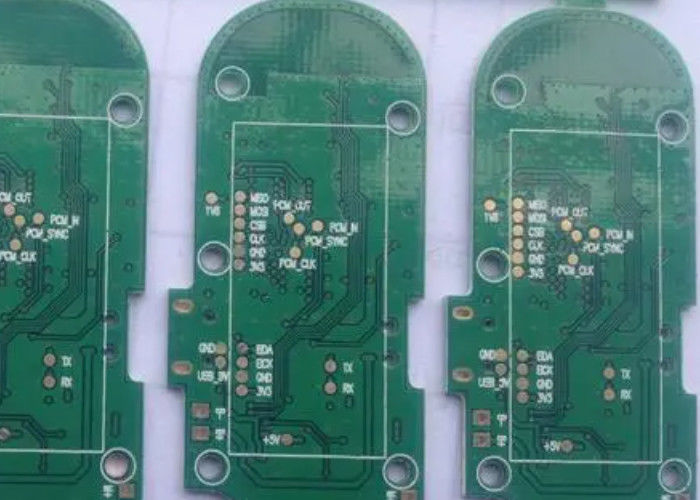
Single-side pcb
The standard PCB board is a general term for all printed boards, which can be divided into single-layer boards or multi-layer boards as required. The substrate of the board itself is made of an insulating, non-bendable material. You can see that on the surface
The wiring material is copper foil. Originally, the copper foil is covered on the whole board, but in the manufacturing process, the middle part is etched away, and the remaining part becomes a network of small lines. These lines are called conductors
pattern) or wiring, and used to provide circuit connection of parts on PCB. The PCB board is V-CUT
PCB, that is, there are several boards in a board, not a single out. Plate shipment is roughly the same, mold out of the plate when a four, six, eight and so on. Not single out to facilitate the production of SMD components.
Incoming material detection => PCB side A screen printing solder paste (spot patch glue) => patch => drying (curing) => reflow welding => cleaning => plug-in => wave soldering => cleaning => detection => repair
Single layer board is the most basic pcb type board, also called single panel, because the wire only appears on one side, so we call this pcb board single panel.
| Copper Thickness | 1oz~3oz,0.5-5 Oz |
| Board Thickness | 1.6mm, 0.5~3.2mm, 0.2-3.0mm, 0.3~2.5mm, 2.0mm |
| Min. Hole Size | 0.25mm, 0.1mm, 0.2 Mm, 0.15-0.2mm, 0.1mm-1mm |
| Min. Line Spacing | 0.003", 4mil, 0.2mm, 0.15mm, 0.1mm4mil) |
| Application | Electronics Device, Consumer Electronics, Electronical Products, Industrial, And So On |
| Layer | 1~20 Layers, 1-24layers |
| Base Material | FR4, Aluminium, TG, Rogers, CEM-1 |
| Min. Line Width | 3mi, 4mil, 0.1mm, 0.1mm(Flash Gold)/0.15mm(HASL), 0.1 0mm |
| Surface Finishing | HASL, OSP, ENIG, HASL Lead Free, Immersion Gold |
| Product Name | Printed Circuit Board, 94V0 PCB Design / PCB Manufacturing |
| Solder Mask | Blue, Green. Red. Blue. White. Black.Yellow, Green/black/white/red/blue Etc., |
| Rohs | Lead free |
Single-Sided pcb Smt
SMT basic process elements include: screen printing (or dispensing), mounting (curing), reflow soldering, cleaning, testing, repair
1. Screen printing: Its function is to leak solder paste or patch glue onto the PCB pad to prepare for the welding of components. The equipment used is screen printing machine (screen printing machine), located at the front end of the SMT line.
2, dispensing: it is to drop the glue to the fixed position of the PCB board, its main role is to fix the components to the PCB board. The equipment used is the dispensing machine, which is located at the front end of the SMT production line or behind the testing equipment.
3. Mounting: Its function is to accurately install the surface assembly components to the fixed position of PCB. The equipment used is the SMT machine, which is located behind the screen printing machine in the SMT production line.
4, curing: its role is to melt the patch glue, so that the surface assembly components and PCB board firmly bonded together. The equipment used is the curing furnace, which is located behind the SMT machine in the SMT line.
Our Advantages:
1. Program and functional test and package by Free.
2. High quality: IPC-A-610E standard, E-test, X-ray, AOI test, QC, 100% functional test.
3. Professional service: PCB/FPC/Aluminium Making, SMT, DIP, Component Sourcing, OEM with 21 years experience.
4. Certifications: UL, 94v-0, CE, SGS, FCC, RoHS, ISO9001, ISO14001,IATF16949
![]()
![]()
![]()
![]()
Kerongda is a PCB manufacturer, providing turnkey and partial turnkey printed circuit board assembly services.We can produce customized PCB board and PCBA for you ,PCB solder mask color ,material, thickness etc... all can be chosed as your demands.
Contact Person: Wang
Tel: 18006481509