|
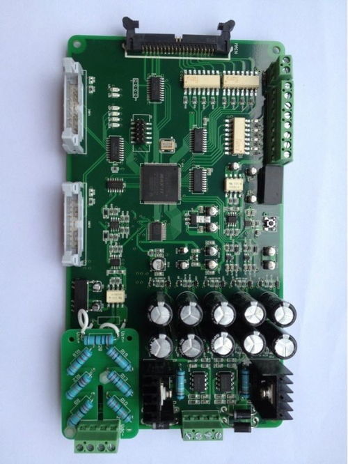
Product Details:
|
| Copper Thickness: | 1oz,0.5-2.0 Oz,1-3oz,0.5-5oz,0.5-4oz | Base Material: | 1.6-2.0mm |
|---|---|---|---|
| Product Name: | Printed Circuit Board, 94V0 PCB Design / PCB Manufacturing / PCB Assembly In China, Double Sided PCB, 2 Layer HASL 94V0 FR4 PCB Manufacturer, Electronic Pcb Assembly | Type: | Customizable, Electronic Board, Electronic PCB Assembly, Alarm Pcb Board |
| Item: | ODM OEM LED PCBA, 2 Layer Pcb, Keyboard Pcb Assembly, Custom Circuit Board | Service: | One-stop Service, PCB&PCBA, ODM And OEM |
| High Light: | through hole pcb assembly process,4 layer through hole pcb,through hole circuit board |
||
SMT basic process elements include:
screen printing (or dispensing), mounting (curing), reflow soldering, cleaning, testing, repair
1. Screen printing: Its function is to leak solder paste or patch glue onto the PCB pad to prepare for the welding of components. The equipment used is screen printing machine (screen printing machine), located at the front end of the SMT line.
2, dispensing: it is to drop the glue to the fixed position of the PCB board, its main role is to fix the components to the PCB board. The equipment used is the dispensing machine, which is located at the front end of the SMT production line or behind the testing equipment.
DIP
1,The process of DIP processing is: putting in the hole →AOI→ wave soldering → cutting pin →AOI→ correction → washing → quality inspection.
2,After wave soldering, The products will be will scanned by AOI equipment to ensure that no error occurs.
Our Advantages:
1. Program and functional test and package by Free.
2. High quality: IPC-A-610E standard, E-test, X-ray, AOI test, QC, 100% functional test.
3. Professional service: PCB/FPC/Aluminium Making, SMT, DIP, Component Sourcing, OEM with 21 years experience.
4. Certifications: UL, 94v-0, CE, SGS, FCC, RoHS, ISO9001, ISO14001,IATF16949
| No. | Types Of Assembly | File Format | Component Footprinr | Component Package | Testing Produres | Produres | Others |
| 1 | SMT ASSEMBLY | Gerber RS-274X | 0201,0402,0603... | Reels Package | Visual Inspection | Lead-Free(Rohs) | Custom Reflow Profile |
| 2 | SMT & THT Assembly | BOM(.xls,.csv,.xlsx) | BGA,QFN,QFP,PLCC | Cut Tape Package | X-Ray Inspection | Leaded Solder | Standard Reflow Profile |
| 3 | 2 sided SMT,THT Assembly | Pick-N-Place/XY file | SOIC,POP...Connectors | Tube and Tray | AOI,ICT(In-Circuit Test) | Reflow Soldering | Smallest Size:0.2"x0.2" |
| 4 | Mixed Assembly | ... | Small Pitch of 8 Mils | Loose parts and bulk | Functional Testing | Wave Soldering | Largest Size:15"x"20 |
![]()
![]()
![]()
![]()
Contact Person: Wang
Tel: 18006481509