English
English
French
German
Italian
Russian
Spanish
Portuguese
Dutch
Greek
Japanese
Korean
Arabic
Hindi
Turkish
Indonesian
Vietnamese
Thai
Bengali
Persian
Polish
Request A Quote
|
Search
Home
Products
About Us
Factory Tour
Quality Control
Contact Us
News
Cases
Sorry! This product is no longer available.
Let's see if there are any related products that interest you
Recommended Products
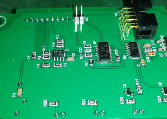
Custom Smt Tht with Green Solder Mask V Cut Board Cutting and 3.0mil Min Line
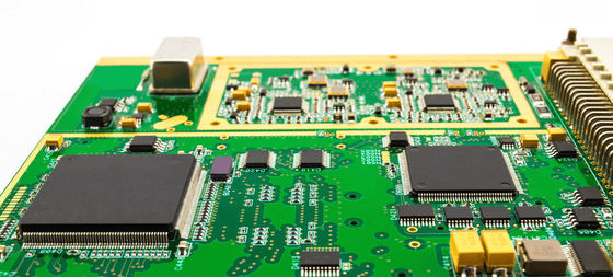
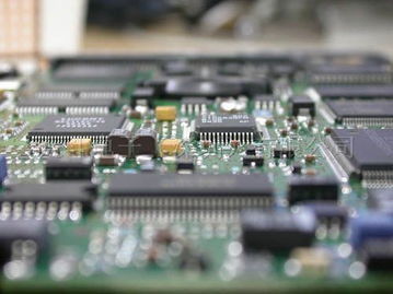
0.5-4 oz Cu Weight ROHS Compliant PCB Assembly Service with 14 SMT Lines
Precision Green/Red 1OZ Copper SMT for YS100 Machine KLA-M5890-07
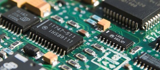
Top/Bottom SMT PCB Assembly with 1OZ Copper Green/Red Color 4mil Spacing
FR-4 1OZ PCB SMT PCBA Assembly White Silkscreen with 3mil Minimum Line Space Green Solder Mask
1OZ Green/Red SMT PCB Assembly for YS100 Machine Top/Bottom Mounting 4mil Spacing Plugging Vias 0.2-0.8mm
White Silkscreen Precision 4mil 3mil 1OZ Copper PCB Assembly for YS100 SMT Machine
0.10mm Minimum Hole Diameter PCB for Precise and Accurate Applications
±10% Board Thickness Tolerance Quick Turn PCB Assembly with and IPC Class 2 Standard
0.2mm-4.0mm Thickness SMT PCB with 0.10mm Minimum Hole Diameter
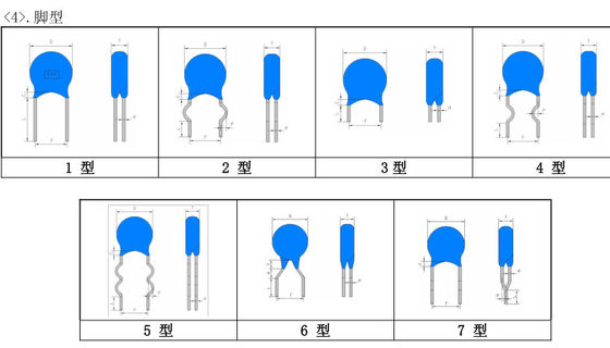
Y2 472M 4700UF 250V P7.5Y5V Very Hight Tension X1 Y1 X2 Y2 Ac Ceramic Capacitors
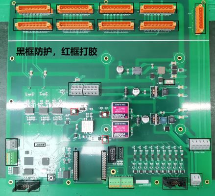
Quick Turn SMT PCBA Assembly with Green Solder Masked
FR-4 Material SMT PCB Assembly For Plugging Vias Capability 0.2-0.8mm And Green Solder Mask
Top Mounting Type PCB With Minimum Hole Size Of 0.2mm At Competitive
FR-4 Material SMT PCB Assembly for YS100 Machine in Categary
Streamline Your Production With SMT Copper Thickness 1OZ From Trusted
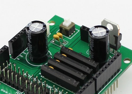
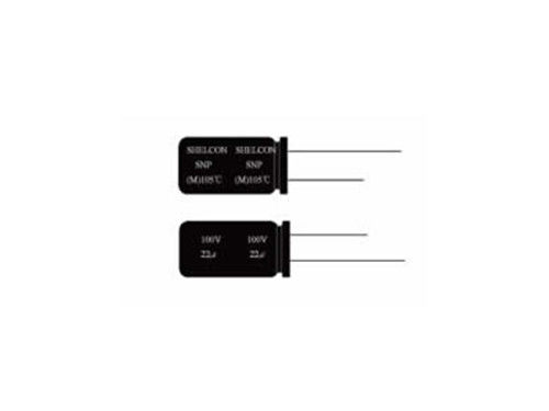
SMT Aluminum Electrolytic Capacitor High Cost Performance
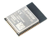
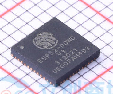
Wifi Module ESP32 Communication Module 4G 5G Module Integrated Circuit Chip
ESP32-D0WD IC CHIP 32Mbits SPI Flash 40MHz Crystal Oscillator Onboard / U.FL / IPEX A
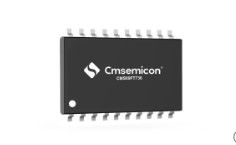
CMS89FT73x EEPROM IC CHIP 16MHz 8K Flash 256Bytes RAM 320Bytes Touch RAM