|
Product Details:
|
| Material: | FR-4 | Color: | Green, Customized Color, Blue On Your Request |
|---|---|---|---|
| Copper Thickness: | 1oz,0.5-2.0 Oz,1-3oz,0.5-5oz,0.5-4oz | Board Thickness: | 1.6mm, 0.5~3.2mm, 0.2-3.0mm, 0.3~2.5mm, 2.0mm |
| Min. Line Width: | 3mi, 4mil, 0.1mm, 0.1mm(Flash Gold)/0.15mm(HASL), 0.1 0mm | Application: | Electronics Device, Consumer Electronics, Electronical Products, Industrial, And So On |
| Highlight: | 8 layer pcb motherboard,making multilayer pcb,multilayer pcb production |
||
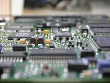
Advantages of multilayer circuit boards
1, the multi-layer circuit board assembly density is high, the size is small, with the volume of electronic products is getting smaller and smaller, the function of PCB circuit board is also put forward higher requirements, the demand for multi-layer circuit board is also increasing.
2, the selection of multi-layer PCB circuit board laying line is convenient, the length of the laying line is greatly shortened, the laying line between the electronic components is reduced, but also improve the data signal transmission rate.
| Copper Thickness | 1oz~3oz,0.5-5 Oz | Base Material | FR4, Aluminium, TG, Rogers, CEM-1 |
| Board Thickness | 1.6mm, 0.5~3.2mm, 0.2-3.0mm, 0.3~2.5mm, 2.0mm | Min. Line Width | 3mi, 4mil, 0.1mm, 0.1mm(Flash Gold)/0.15mm(HASL), 0.1 0mm |
| Min. Hole Size | 0.25mm, 0.1mm, 0.2 Mm, 0.15-0.2mm, 0.1mm-1mm | Surface Finishing | HASL, OSP, ENIG, HASL Lead Free, Immersion Gold |
| Min. Line Spacing | 0.003", 4mil, 0.2mm, 0.15mm, 0.1mm4mil) | Product Name | Printed Circuit Board, 94V0 PCB Design / PCB Manufacturing |
| Application | Electronics Device, Consumer Electronics, Electronical Products, Industrial, And So On | Solder Mask | Blue, Green. Red. Blue. White. Black.Yellow, Green/black/white/red/blue Etc., |
| Layer | 1~20 Layers, 1-24layers | Rohs | Lead free |
![]()
![]()
![]()
Contact Person: Wang
Tel: 18006481509