|
Product Details:
|
| Product Name: | Printed Circuit Board, 94V0 PCB Design / PCB Manufacturing / PCB Assembly In China, Double Sided PCB, 2 Layer HASL 94V0 FR4 PCB Manufacturer, Electronic Pcb Assembly | Material: | FR-4 |
|---|---|---|---|
| Board Thickness: | 1.6mm, 0.5~3.2mm, 0.2-3.0mm, 0.3~2.5mm, 2.0m | Type: | Customizable, Electronic Board, Electronic PCB Assembly, Alarm Pcb Board |
| Application: | Electronics Device, Consumer Electronics, Electronical Products, Industrial, And So On | Color: | Green, Customized Color, Blue On Your Request |
| Layers: | 1-28 | Min. Hole Size: | 0.25mm, 0.1mm, 0.2 Mm, 0.15-0.2mm, 0.1mm-1mm |
| Highlight: | outsource electronics assembly,prototype electronics assembly,ems pcb manufacturer |
||
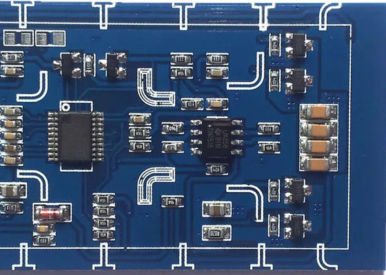
SMT
SMT patch processing will purchase components according to BOM, BOM provided by customers and confirm the PMC plan of production. After the preparatory work is completed, we will start SMT programming, manufacture laser steel mesh and solder paste printing according to the SMT process.
The components will be mounted on the circuit board through SMT mounter, and online AOI automatic optical detection will be carried out if necessary. After testing, the perfect reflow furnace temperature curve is set to let the circuit board flow through reflow welding.
After the necessary IPQC inspection, the DIP material can then be passed through the circuit board using the DIP process and then through wave soldering. Then it is time to carry out the necessary post-furnace process.
After all the above processes are completed, QA will conduct a comprehensive test to ensure product quality.
Advantages of single layer circuit board
(1) Low cost: The manufacturing cost of single-layer PCB board is relatively low, because only one layer of copper foil and one layer of substrate are needed, and the manufacturing process is relatively simple.
(2) Easy production: Compared with other structural types of PCB board, the production method of single-layer PCB board is relatively simple, only need to carry out single-side wiring and single-layer corrosion, so the production difficulty is low.
(3) High reliability: Single-layer PCB board does not have multi-layer wiring and connection, so it is not easy to short-circuit and interference problems, with high reliability.
(4) Suitable for simple circuit: single-layer PCB board is suitable for simple circuit design, such as LED lights, sound, etc., can meet most of the low complexity of the circuit requirements.
| Turnkey PCBA | PCB+components sourcing+assembly+package | ||||
| Assembly details | SMT and Thru-hole, ISO lines | ||||
| Lead Time | Prototype: 15 work days. Mass order: 20~25 work days | ||||
| Testing on products | Flying Probe Test, X-ray Inspection, AOI Test, functional test | ||||
| Quantity | Min quantity: 1pcs. Prototype, small order, mass order, all OK | ||||
| Files we need | PCB: Gerber files(CAM, PCB, PCBDOC) | ||||
| Files we need | Components: Bill of Materials(BOM list) | ||||
| Files we need | Assembly: Pick-N-Place file | ||||
| PCB panel Size | Min size: 0.25*0.25 inches(6*6mm) | ||||
| Max size: 20*20 inches(500*500mm) | |||||
| PCB Solder Type | Water Soluble Solder Paste, RoHS lead free | ||||
| Components details | Passive Down to 0201 size | ||||
| Components details | BGA and VFBGA | ||||
| Components details | Leadless Chip Carriers/CSP | ||||
| Components details | Double-sided SMT Assembly | ||||
| Components details | Fine Pitch to 0.8mils | ||||
| Components details | BGA Repair and Reball | ||||
| Components details | Part Removal and Replacement | ||||
| Component package | Cut Tape,Tube,Reels,Loose Parts | ||||
| PCB assembly | Drilling-----Exposure-----Plating-----Etaching & Stripping-----Punching-----Electrical Testing-----SMT-----Wave Soldering-----Assembling-----ICT-----Function Testing-----Temperature & Humidity Testing | ||||
1, the multi-layer circuit board assembly density is high, the size is small, with the volume of electronic products is getting smaller and smaller, the function of PCB circuit board is also put forward higher requirements, the demand for multi-layer circuit board is also increasing.
2, the selection of multi-layer PCB circuit board laying line is convenient, the length of the laying line is greatly shortened, the laying line between the electronic components is reduced, but also improve the data signal transmission rate.
![]()
![]()
![]()
Contact Person: Wang
Tel: 18006481509